Tales of FPGA - Road to SDRAM - E01
Posted on July 25, 2022 in hacks
This post is the first one of a serie, which aims at providing a simple working example of a design that can reliably access the SDRAM chip on a Digilent Arty S7 FPGA development board. Indeed, although this board has been out for quite some time now, such a design seems practically impossible to find on the 'net, for reasons we will try to analyze.
I also mean this serie to be an introduction to FPGA for people who have little idea what they actually are nor how they work. So, even if you do not care about accessing SDRAM on that particular board, you may find it an interesting read. In fact, my interest in FPGA owes a lot to the fact that they help understand the inner working of a CPU, a RAM, and any modern computer.
Arty S7?
The Arty S7 is an FPGA development board based upon Xilinx' Spartan-7 series of FPGA chips. It is a cost-effective design packing an FPGA chip, DDR3L memory, buttons, leds, I/O and expansion ports... everything you need to experiment with an FPGA at a reasonable cost (around USD 100.00).
![]()
In a way, it is similar to an Arduino board, with the CPU replaced by the FPGA chip.
And what is an FPGA chip?
An FPGA is a Field Programmable Gate Array: a semiconductor device based around a matrix of configurable logic blocks, connected via programmable interconnects. The most basic logic block would be, for instance, an AND gate:
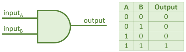
When any of the gate inputs change, the output is adjusted, after a short inevitable delay. This type of gate can be implemented with a few transistors, and along with the other OR, XOR... gates they are the basic elements of all silicon-based operations.
In reality, FPGA do not implement AND gates, and their most basic logic block would rather be a 2-bit look-up table, or LUT2. It also has two inputs and one output, and updates its output according to its inputs. But the value of the output is specified by a 2x2 logic table. This way, one single block can be configured to be an AND, OR, XOR... gate.
And then there are LUT4, LUT6... which follow the same principle only with more inputs. You would also find flip-flops which can latch a stable state on a clock signal, oscillators, some type of memories, etc. that you can all configure in the same way one configures the logic table of a LUT2.
All these blocks are layed out in precise positions on the die of the FPGA chip. And then, there is an interconnect layer which can be configured to wire (pratically) any block input or output with any other block input or output. So you could configure a LUT2 as an AND gate, and wire its output to the input of another LUT2 configured as an OR gate, etc.
The whole configuration is represented as a blob of binary data which needs to be fed to the FPGA before it can operates. Traditionally, some additional hardware on the development board handle this process and read this blob from Flash memory, or allow the developer to upload it via an USB link.
Taking Control
FPGA manufacturers provide tools and development environments that let users configure their chips. Xilinx, a major FPGA actor owned by AMD, even have several of them, the most popular (and having a free edition) being the Vivado IDE. These tools support various description languages such as VHDL or Verilog or its SystemVerilog evolution. These languages are used to specify the FPGA internal configuration, as a set of text files.
The major difference with traditional programming languages is that all these elements and signals and connections operate concurrently. An FPGA design is a massively parallel thing.
This post is certainly not a VHDL nor Verilog tutorial. Let us just say that it all begins with a module which has inputs and outputs (connected to the actual external pins of the FPGA), along with internal signals, and defines connections between these signals. The following module would for instance act as an AND gate:
module and_gate (
    input logic in_0,
    input logic in_1,
    output logic out
);

    LUT2 #(
        .INIT (4'b1000)    // define the logic table
    )
    LUT2_inst (
        .I0 (in_0),        // wire module input in_0 to LUT2 input I0
        .I1 (in_1),        // wire module input in_1 to LUT2 input I1
        .O (out)           // wire LUT2 output 0 to module output out
    );

endmodule
The LUT2 logic table is documented as being a 4-bit value with the higher-rank bit (left-most) representing the output value when both inputs are 1, and thus, our LUT2 will act as an AND gate.
Vivado can then "compile" this design, provided that you also tell it how to wire the inputs and outputs of the module. For instance, inputs could be wired to buttons, and outputs to LEDs. The compiler will determine which LUT2 to use on the board, and produce the FPGA configuration binary blob, that Vivado can feed to the board via USB. There, done, our first design!
However, Verilog (the language) is way more clever than that. It does not merely "compile" the design, but synthesize it. It can infer which blocks to use, depending on logical syntax. Noone would ever write a module such as the one above. Instead, one would simply write the following code:
module and_gate (
    input logic in_0,
    input logic in_1,
    output logic out
);

    assign out = in_0 & in_1;

endmodule
The tools would determine that you are assigning out to be the logical AND between in_0 and in_1, and that the most convenient block to achieve this is a LUT2. It could as well understand that you want to add two 8-bit numbers, and select and wire together the relevant blocks: a large combination of LUTs maybe, unless the FPGA provides some built-in adder blocks.
In fact, most designs only explicitly instantiate complex blocks (clocks, memories...) but usually let the language deal with the rest (LUTs, flip-flops...).
The Obligatory LED Blinker
The following module accepts a clock logic signal as an input, produces a LED logic signal as an output, and would toggle that LED signal periodically, thus blinking the LED.
module testbench (
    input  logic clk,   // the logical input clock signal
    output logic led    // the logical output signal controlling the LED
);
    localparam COUNT_WIDTH = 8;

    // count and next_count are a multiple-bits signals of width COUNT_WIDTH
    var logic [COUNT_WIDTH-1:0] count, next_count;

    initial count = 0;

    // the next_count signal continuously updates to be count + 1
    // it's only bits: when count reaches its max value, it wraps to zero
    assign next_count = count + 1;

    // the led signal continuously reflects the highest bit of the count signal
    assign led = count[COUNT_WIDTH-1];

    // on each raising edge of the clk signal,
    // update the count signal with its next value
    always @ (posedge clk) count <= next_count;

endmodule
Note:
- Things defined as
varare internal signals, similar to a wire connecting blocks. - The
assignstatement means: the signal on the left-hand side of the=sign should constantly reflect the result of the expression on the right-hand site. They would probably be implemented with LUTs. - The
always @ (posedge clk)means: the signals on the left-hand side of the<=signs should be updated to reflect the result of the expressions on the right-hand sign, on each raising edge of theclksignal. They would probably be implemented with a combination of LUTs and flip-flops. countis an array of bits, containingCOUNT_WIDTHbits. It is constantly incremented. IfCOUNT_WITHis 2, thencountwould be00,01,10,11,00,01, etc. and its highest bit would be 0 half of the time, and 1 the other half.
Assuming you tell Vivado to wire the clk input to the on-board physical clock, and the led output to a LED, and if you configure COUNT_WIDTH correctly as per the clk signal frequency... this should blink the LED on the board.
Or Maybe Not
And then what? There is no way you can plug a debugger into the FPGA. Remember, there is no "code" executing: everything is happening at hardware, electrical level, and you cannot inspect what happens at silicon level. For very large designs, Xilinx does provide some methods to add analysis features to your design and actually extract the value of some signals, but they are rather cumbersome and intrusive.
It is all a black box.
All you can do is go back to your design, and think.
On the other hand, FPGA tools such as the Vivado IDE can simulate a design, i.e. emulate the complete behavior of the elements, all within the PC memory. Vivado comes with a virtual logic analyzer, which shows the signals in details. Here is an example of waveforms it can produce.
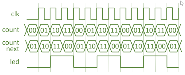
Such an analysis will help you figure out your logical errors, to the point that the simulation is correct. And then... If the code does not have syntax errors, and the design simulates correctly, everything should run successfully on hardware too.
Let us stop on that (naïvely?) positive note here.
To be continued!
There used to be Disqus-powered comments here. They got very little engagement, and I am not a big fan of Disqus. So, comments are gone. If you want to discuss this article, your best bet is to ping me on Mastodon.